About Shennan
Solutions
Product Technology
Investor Relations
Social responsibilities
Join Us


FC-CSP基板
WB-CSP
eMCP基板
Memory-MSD基板
RF基板
MEMS-SEN基板
MEMS-MIC基板

Features :
● 2~6 layers
● Package type : FC
● Typic Line Width/Space : 12/12μm-25μm/25μm
Applications:
High end AP packaging ( Applied in smart phone, PC, and Multimedia equipment, etc).

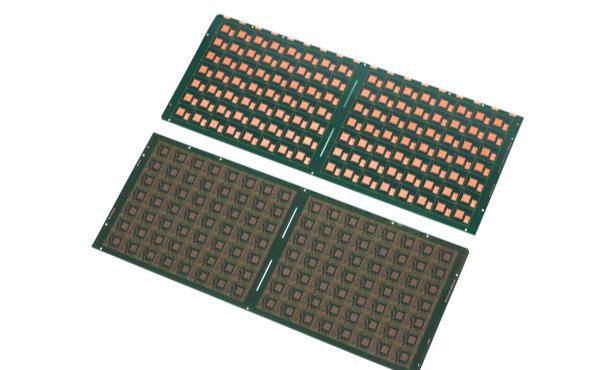
Features :
● 2~6 layers
● Package type : WB
● Package Size: 3*3mm - 23*23mm
● Thickness : 0.11mm-0.56mm
● Typic Line Width/Space : 25/25μm-40μm/40μm
Applications: AP packaging (Applied in mobile phone, PC, and Multimedia equipment, etc).

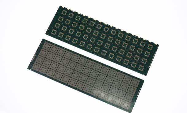
Features :
● 2,3,4 layers
● Typical BF Pitch:70-90μm
● Strict Solder resist Flatness
Surface finish:电金+OSP
Applications:
eMMC or eMCP memory IC packaging( Applied in smart phone, PC, and server etc).

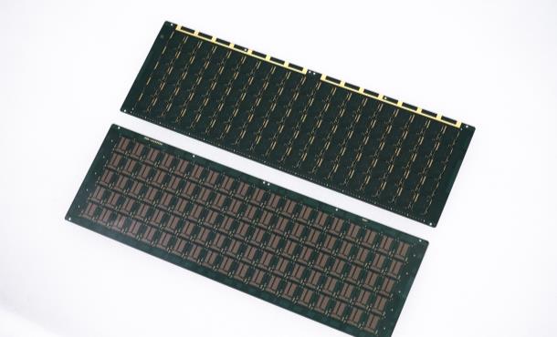
Features :
● 2~4 layers
● Board thickness:130um
● Typic BF Width/Space : 75μm~100μm
● Printing ink type:Black oil
● Surface finish:Hard gold,Electroplated Soft Gold
Applications:
Memory module packaging ( Applied in Navigation, Digital Camera, PDA, Laptop ).

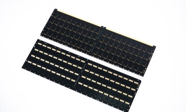
Features :
● 2~8 Layer
● Surface finish: Ni/Au( Bussless), ENEPIG, OSP.
● Tighten pattern dimension and thickness conformity
● Tighten layer registration control
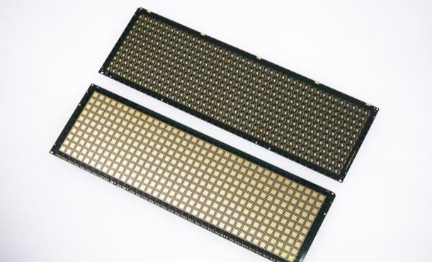
Applications:
RF module packaging (Applied in Smart phones ,wearable devices and IOT application and PC, etc).

Features :
● 2Layer
● Thin board: 100μm or 130μm
● Fine pitch pattern
● Surface finish: Ni/Au( Bussless), ENEPIG, OSP.
● Strict Warpage control ≤0.9mm

Applications:
MEMS-sensor Module packaging (Applied in Smart phone, wearable device, Automotive, Medical instrument)

Features :
● 2,4,6Layer
● Embedded Capacitor and Resistor
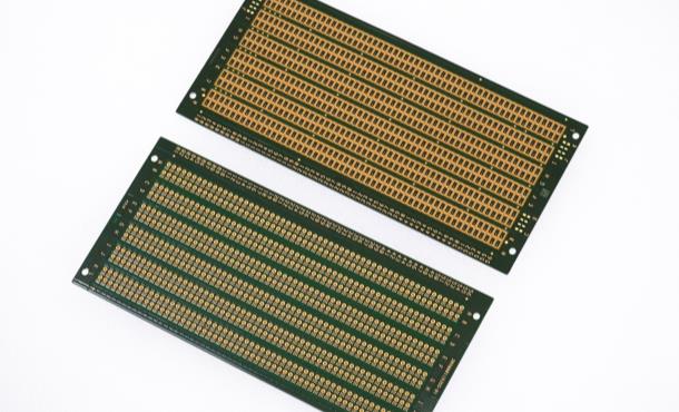
Applications:
MEMS-microphone module packaging (Applied in smart phone,intelligent sound box, wearable device and PC etc).
FC-CSP基板
WB-CSP
eMCP基板
Memory-MSD基板
RF基板
MEMS-SEN基板
MEMS-MIC基板

Features :
● 2~6 layers
● Package type : FC
● Typic Line Width/Space : 12/12μm-25μm/25μm

Applications:
High end AP packaging ( Applied in smart phone, PC, and Multimedia equipment, etc).

Features :
● 2~6 layers
● Package type : WB
● Package Size: 3*3mm - 23*23mm
● Thickness : 0.11mm-0.56mm
● Typic Line Width/Space : 25/25μm-40μm/40μm

Applications: AP packaging (Applied in mobile phone, PC, and Multimedia equipment, etc).

Features :
● 2,3,4 layers
● Typical BF Pitch:70-90μm
● Strict Solder resist Flatness
Surface finish:电金+OSP

Applications:
eMMC or eMCP memory IC packaging( Applied in smart phone, PC, and server etc).

Features :
● 2~4 layers
● Board thickness:130um
● Typic BF Width/Space : 75μm~100μm
● Printing ink type:Black oil
● Surface finish:Hard gold,Electroplated Soft Gold

Applications:
Memory module packaging ( Applied in Navigation, Digital Camera, PDA, Laptop ).

Features :
● 2~8 Layer
● Surface finish: Ni/Au( Bussless), ENEPIG, OSP.
● Tighten pattern dimension and thickness conformity
● Tighten layer registration control

Applications:
RF module packaging (Applied in Smart phones ,wearable devices and IOT application and PC, etc).

Features :
● 2Layer
● Thin board: 100μm or 130μm
● Fine pitch pattern
● Surface finish: Ni/Au( Bussless), ENEPIG, OSP.
● Strict Warpage control ≤0.9mm

Applications:
MEMS-sensor Module packaging (Applied in Smart phone, wearable device, Automotive, Medical instrument)

Features :
● 2,4,6Layer
● Embedded Capacitor and Resistor

Applications:
MEMS-microphone module packaging (Applied in smart phone,intelligent sound box, wearable device and PC etc).
Copyright © Shennan Circuits Company Limited. All rights reserved.
 86-755-89300000
Technical support: E-tionCommunication
